
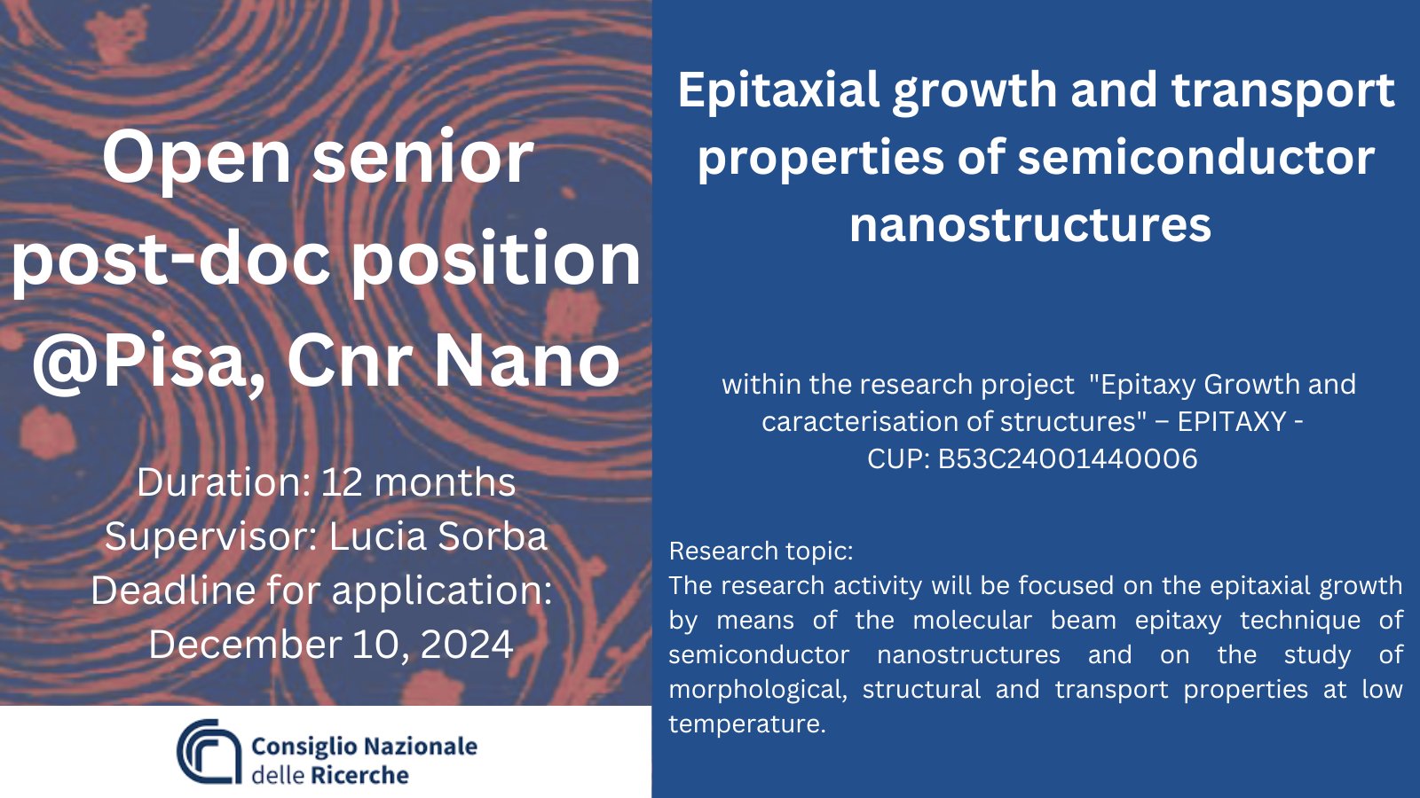
Postdoc Opportunity -Semiconductor Structures: The Istituto Nanoscienze, Consiglio Nazionale delle Ricerche is inviting applications for a Professionalizing Research Fellowship in the area of “Epitaxy: Growth and Characterization of Semiconductor Structures.” The fellowship, under the supervision of Dr. Lucia Sorba, offers the opportunity to engage in advanced research within the autonomous project “Growth and Characterization of Structures – EPITAXY.”
Postdoc Opportunity – Epitaxy: Growth and Characterization of Semiconductor Structures
Designation: Professionalizing Research Fellowship
Research Area: Epitaxy: Growth and Characterization of Semiconductor Structures
Location: Pisa, Italy
Eligibility/Qualification:
- Master’s degree in Physics, Materials Science and Nanotechnology, Materials Engineering, or related field
- Proficiency in semiconductor growth, fabrication techniques, and transport measurements
- Proficiency in English; knowledge of Italian required for non-Italian candidates
Job Description:
The successful candidate will be engaged in the detailed investigation and experimentation related to epitaxial growth and characterization of semiconductor structures. This entails working within the framework of the self-financed project “Growth and Characterization of Structures – EPITAXY,” focusing on advancing the scientific understanding in this specialized field.
How to Apply:
Interested candidates should submit their applications via Certified Electronic Mail to protocollo.nano@pec.cnr.it. Non-Italian candidates should use the email address nano.recruitment@nano.cnr.it. Further details and application templates can be accessed at https://www.urp.cnr.it/system/files/2024-10/Bando-NANO-AR-034-2024-PI_signed.pdf.
Deadline for Application: December 10, 2024
This fellowship offers a unique opportunity to contribute to cutting-edge research in the field of semiconductor structures and epitaxy under the guidance of leading experts at the Istituto Nanoscienze. Join us in exploring the forefront of nanoscience and materials engineering in the beautiful city of Pisa, Italy.


")


